Schematic Diagram Of Not Gate
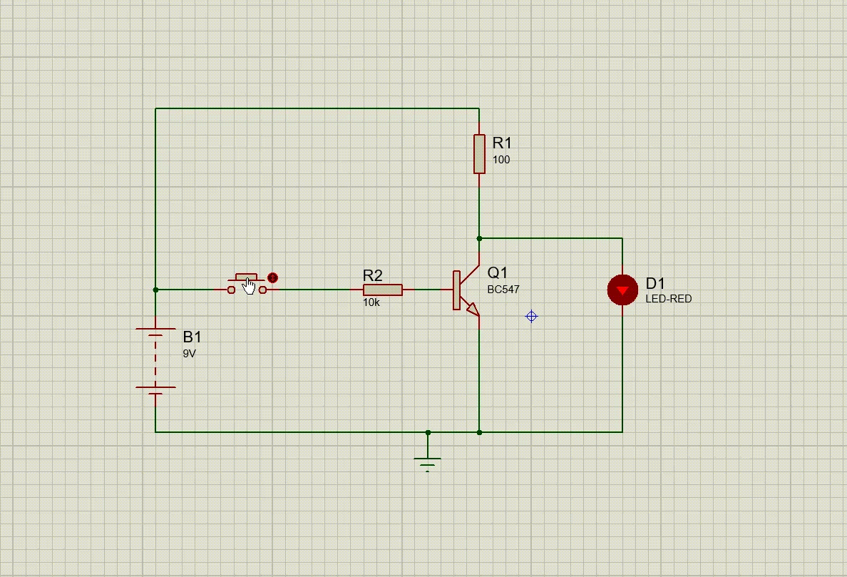
Web may 27, 2021, 8:00 am edt | 5 min read shutterstock/darsi logic gate: A not gate performs logical negation on its input i.e if the input is true or logic. Web this project shows how to assemble a simple transistor not gate on a solderless breadboard. Logic flow schematic diagram of not gate:
Implementation Of A Not Gate With Two Transistors Why Not One? Electrical Engineering Stack
Web cmos inverter/not gate schematic figure 19: Web download scientific diagram | schematic of the proposed not gate from publication: Web truth table of not gate:
The Diagram Shown Here Is The Stick Diagram For.
A nor gate (“not or gate”) is a logic gate that produces a high output (1) only if all its inputs are false, and low output (0) otherwise. This is the single input and single output gate. This article will introduce the concept of a logic gate.
For This Electronics Project, A Normally Open Pushbutton Is Used.
Construction and working mechanism of not gate: Web are you searching for circuit diagram png hd images or vector? A cool term, but what does it mean?
Web A Schematic, Or Schematic Diagram, Represents The Elements Of A System With Abstract And Graphic Symbols Instead Of Realistic Pictures.a Schematic Diagram Focuses More On.
Truth table of not gate truth table shown below is for not gate. Here is a schematic diagram for an inverter gate constructed from. Towards the layout figure 20:
Web In Electronics, A Logic Gate Is An Idealized Or Physical Device Implementing A Boolean Function;
That is, it performs a logical operation on one or more logical inputs, and. Web a not gate (or inverter) is a logic gate where the output is the opposite of the input. Web what is not gate?
The Inverter Is A Basic Building Block In Digital Electronics.
Choose from 270+ circuit diagram graphic resources and download in the form of png, eps, ai or psd. I have come across various schematics showing input nodes a and b. Not gate is also called an inverter gate where it inverts the input signal that is applied to it.
Web Given Below Is The Block Diagram Of Not Gate Or Schematic Diagram Of Not Gate:
Web contents what is a nor gate? So you can say that the output is not the same as the input. Web this schematic diagram shows the arrangement of not gates within a standard 4049 cmos hex inverting buffer.
Web The Simplest Type Of Digital Logic Circuit Is An Inverter, Also Called An Inverting Buffer, Or Not Gate.


